Train Station Display: Difference between revisions
No edit summary |
mNo edit summary |
||
| (27 intermediate revisions by 2 users not shown) | |||
| Line 3: | Line 3: | ||
|type=member | |type=member | ||
|created=13/01/2024 | |created=13/01/2024 | ||
|status= | |location=Metalworking | ||
|image=File: | |repo=[https://github.com/AaronJackson/TrainDepartureBoard-Discord GitHub] | ||
|status=Complete | |||
|image=File:TDB_WorkingABit.jpg | |||
}} | }} | ||
[[Category:Projects]] | [[Category:Projects]] | ||
[[File:Train_Station_Display.jpg|300px|thumbnail]] | |||
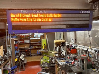
In upstairs metalworking there is a train station display - [https://www.flickr.com/photos/nottinghack/albums/72157629357766648/ photos on flickr]. The display was acquired in October 2011 and hasn't been set up to do anything yet. | In upstairs metalworking there is a train station display - [https://www.flickr.com/photos/nottinghack/albums/72157629357766648/ photos on flickr]. The display was acquired in October 2011 and hasn't been set up to do anything yet. | ||
| Line 13: | Line 18: | ||
The intention is to display messages from discord (and will be named dispcord accordingly). The time section at the bottom will display the channel name, and the main three lines will show the sender and preview of the message. The [[Discord]] bot already relays messages from non-private channels to MQTT. | The intention is to display messages from discord (and will be named dispcord accordingly). The time section at the bottom will display the channel name, and the main three lines will show the sender and preview of the message. The [[Discord]] bot already relays messages from non-private channels to MQTT. | ||
<gallery mode=packed-hover widths=180px> | |||
File:IMG_0496.JPG|Notes|link=File:IMG_0496.JPG | |||
File:Train_Station_Display.jpg|Old Photo|link=File:Train_Station_Display.jpg | |||
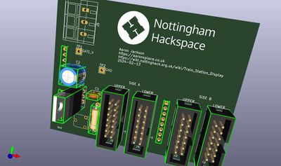
File:TDB_PCB_rendering.jpg|KiCAD Rendering|link=File:TDB_PCB_rendering.jpg | |||
File:Departure_Board.jpg|Railway Departure Board|link=File:Departure_Board.jpg | |||
File:Departure_Board_Shield.jpg|Arduino Shield|link=File:Departure_Board_Shield.jpg | |||
</gallery> | |||
== Parts == | == Parts == | ||
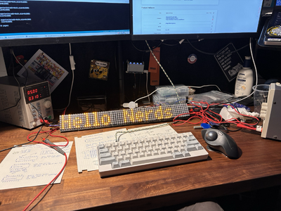
[[File:IMG_0496.JPG|400px]] | |||
=== LED Module === | === LED Module === | ||
| Line 20: | Line 35: | ||
Each LED module contains an 8x7 grid of LEDs. It looks like the module could take 8x8, but maybe the font used wouldn't benefit from having an extra row. | Each LED module contains an 8x7 grid of LEDs. It looks like the module could take 8x8, but maybe the font used wouldn't benefit from having an extra row. | ||
The cathodes of each column are connected together, and the anodes of each row are connected together. At the top and bottom of each module, there is a set of 12 male pins which interface with the module backplane. | |||
<pre> | <pre> | ||
| Line 44: | Line 59: | ||
<pre> | <pre> | ||
Input IDC header | Input IDC header | ||
+-----+ | solder side header side | ||
GND -| o o |- A0 | +-----+ +-----+ | ||
GND -| o o |- A1 | GND -| o o |- A0 GND -| o o |- A6 Strobe | ||
GND -| o o |- A2 | GND -| o o |- A1 Shift2 Di A7 -| o o |- A5 BCD D | ||
? -| o o |- A3 | GND -| o o |- A2 GND -| o o |- A4 BCD C | ||
GND -| o o |- A4 | ? -| o o |- A3 ? -| o o - A3 BCD B | ||
A7 -| o o |- A5 | GND -| o o |- A4 GND -| o o |- A2 BCD A | ||
GND -| o o |- A6 | A7 -| o o |- A5 GND -| o o |- A1 Shift1 Di | ||
+-----+ | GND -| o o |- A6 GND -| o o |- A0 Clock | ||
+-----+ +-----+ | |||
(I'm bad at geometry and will get confused :)) | |||
The Mystery Pin (?) appears to be the 5v power for the UDN2982 source drivers. Maybe they drive this directly from the controller since it allows for blanking of all panels in one go. The mystery pin is daisy chained through all panels in the string. This pin also connects to an unpopulated set of components (LK1, LK2, and LK3) that connect to the logic power supply and ground. | |||
CD74HCT541E | CD74HCT541E | ||
| Line 75: | Line 95: | ||
Y0 - All shift registers, CLOCK | Y0 - All shift registers, CLOCK | ||
Y1 - Bottom shift register of LED Module | Y1 - Bottom shift register of right-most LED Module, Data In | ||
Y2 - BCD Decoder "A" | Y2 - BCD Decoder "A" | ||
Y3 - BCD Decoder "B" | Y3 - BCD Decoder "B" | ||
| Line 81: | Line 101: | ||
Y5 - BCD Decoder "D" | Y5 - BCD Decoder "D" | ||
Y6 - All shift registers, STROBE | Y6 - All shift registers, STROBE | ||
Y7 - Top shift register of LED Module | Y7 - Top shift register of the right-most LED Module, Data In | ||
</pre> | </pre> | ||
| Line 101: | Line 121: | ||
Si is serial in and connects to either Y1 or Y2 of the line driver, or to So of the previous shift register. | Si is serial in and connects to either Y1 or Y2 of the line driver, or to So of the previous shift register. | ||
The BCD decoder (CD4028BCN) is used to turn on/off the columns of all LED modules on an LED module backplane, using a MOSFET (IRF540) and octal source driver UDN2981A. | |||
V | V | ||
| Line 114: | Line 134: | ||
G | G | ||
O O O O O O O O N | |||
0 1 2 3 4 5 6 7 D | |||
+-------------------+ | +-------------------+ | ||
|> UDN2981A | | |> UDN2981A | | ||
+-------------------+ | +-------------------+ | ||
I I I I I I I I V | |||
0 1 2 3 4 5 6 7 s | |||
</pre> | </pre> | ||
=== Backplane Frame === | === Backplane Frame === | ||
| Line 153: | Line 161: | ||
+------------------+ | +------------------+ | ||
</pre> | </pre> | ||
== Bit banging... == | |||
Not had much luck with this yet, but I'm not sure why. | |||
Logic analyzer trace of data lines during power on boot message (can be opened with PulseView) [[File:Train_Departure_Board_Logic_Dump.zip]]. Screenshot for convenience below | |||
[[File:Train_Departure_Board_Logic_Dump.png|700px]] | |||
'''Note:''' In the screenshot it looks like single clock pulses, but each one of those is 8 pulses. Each clock pulse is about 500ns. Arduino using the IO registers is about 250ns, but this is within the timing recommendations for the shift registers, and I've tried reducing the speed too. | |||
'''Unanswered and confusing questions''' | |||
* Why do the two shift registers always receive the same data? My understanding is that one register does the top four rows, and one register does the bottom three rows, but they seem to receive the same data. Very confusing | |||
** They seem to connect to adjacent column inputs on the LED boards, which are then connected together on the LED board itself. This would let you use the same mainboard to drive the LEDs with double the current (with the LED boards we have) or drive double the LEDs (with different LED boards and different data to each shift register). | |||
* Why can't I even get an LED to light up? I leave the shift register data in lines high, multiplex the BCD lines, pulse the clock, do the strobe in the right place (or just leave it high). | |||
* Why does the BCD "D" line only stay high for 68us? And why is it pulsed after each 48 clock pulses? (48 presumably because there are six sets of 8 LED boards?) | |||
** I think this line is for varying the brightness of the display, since enabling it will add 8 to any "enabled" column and result in none turning on. | |||
Update: I think all of these unanswered questions have been answered. | |||
== Early Testing == | |||
In the end the mystery pin turned out to be the problem. It is the voltage used to drive the FETs. Apparently 5v wasn't quite enough and it needs to be slightly higher than the logic level. This voltage can be tweaked to adjust the brightness without multiplexing. | |||
[[File:TDB-EarlyTesting.png|400px]] | |||
=== Working-ish === | |||
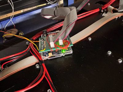
A quick perf-board circuit as an arduino shield let me drive the top two rows. I think I wired something incorrectly though as I wasn't able to get the bottom rows to work at the same time. | |||
[[File:TDB_WorkingABit.jpg|400px]] | |||
[[File:TDB_Proto_Arduino_Sheild.jpg|400px]] | |||
The "mystery pin" (which is the input voltage to the UDN2982 source driver) was being generated with a potential divider. I knew this might cause an issue since the mosfets will draw a bit of current between the gate and drain, but it was much worse than I thought. | |||
=== A PCB... === | |||
Waiting for this to arrive but sent off to JLCPCB. The potential divider has been replaced with an LM317 voltage regulator and small trim pot. This should work a bit better. hopefully... | |||
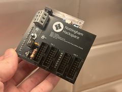
[[File:TDB_PCB_rendering.jpg|400px]] | |||
Sources are on GitHub https://github.com/AaronJackson/TrainDepartureBoard-Discord | |||
== Hooking up to Discord... == | |||
The next steps... It's a work in progress | |||
Latest revision as of 14:31, 21 April 2024
| Train Station Display | |
|---|---|
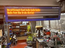 | |
| Primary Contact | Asj |
| Created | 13/01/2024 |
| Location | Metalworking |
| GitHub / Repo | GitHub |
| Status | Complete |
| Type | Members Project |
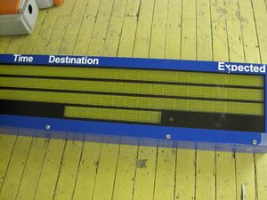
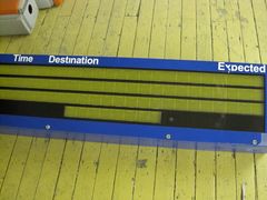
In upstairs metalworking there is a train station display - photos on flickr. The display was acquired in October 2011 and hasn't been set up to do anything yet.
The display seems to use 4-wire MODBUS, and has some DIP switches to configure it's ID (currently 20, as displayed at startup). The registers and commands will be completely undocumented, so bitbanging the display seems like an easier idea.
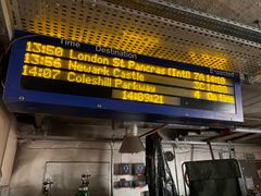
The intention is to display messages from discord (and will be named dispcord accordingly). The time section at the bottom will display the channel name, and the main three lines will show the sender and preview of the message. The Discord bot already relays messages from non-private channels to MQTT.
-
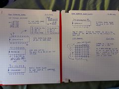
Notes
-
Old Photo
-
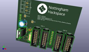
KiCAD Rendering
-
Railway Departure Board
-
Arduino Shield
Parts
LED Module
Each LED module contains an 8x7 grid of LEDs. It looks like the module could take 8x8, but maybe the font used wouldn't benefit from having an extra row.
The cathodes of each column are connected together, and the anodes of each row are connected together. At the top and bottom of each module, there is a set of 12 male pins which interface with the module backplane.
p4 n n p3 n n p2 n n p1 n n

o o o o o o o o      row 1 (via p1 top)
o o o o o o o o      row 2 (via p2 top)
o o o o o o o o      row 3 (via p3 top)
o o o o o o o o      row 4 (via p4 top)

o o o o o o o o      row 1 (via p1 bottom)
o o o o o o o o      row 2 (via p2 bottom)
o o o o o o o o      row 3 (via p3 bottom)
x x x x x x x x      row 4 (via p4 bottom, not populated)

p4 n n p3 n n p2 n n p1 n n
LED Module Backplane
Each backplane holds 8 LED modules. There is a 14 pin IDC header on the right of each board, these go to a CD74HCT541E octal buffer.
Input IDC header

   solder side                             header side
     +-----+                                  +-----+
GND -| o o |- A0                         GND -| o o |- A6  Strobe
GND -| o o |- A1              Shift2 Di  A7  -| o o |- A5  BCD D
GND -| o o |- A2                         GND -| o o |- A4  BCD C
?   -| o o |- A3                         ?   -| o o  - A3  BCD B
GND -| o o |- A4                         GND -| o o |- A2  BCD A
 A7 -| o o |- A5                         GND -| o o |- A1  Shift1 Di
GND -| o o |- A6                         GND -| o o |- A0  Clock
     +-----+                                  +-----+

(I'm bad at geometry and will get confused :))

The Mystery Pin (?) appears to be the 5v power for the UDN2982 source drivers. Maybe they drive this directly from the controller since it allows for blanking of all panels in one go. The mystery pin is daisy chained through all panels in the string. This pin also connects to an unpopulated set of components (LK1, LK2, and LK3) that connect to the logic power supply and ground.

CD74HCT541E

    V O
    c E Y Y Y Y Y Y Y Y     <---- outputs
    c 2 0 1 2 3 4 5 6 7
  +---------------------+
  |>   CD74HCT541E      |
  +---------------------+
    O A A A A A A A A G
    E 0 1 2 3 4 5 6 7 N     <--- inputs
    1                 D
Some of the output lines from the line driver go to the shift registers, while others go to a BCD decoder. Each LED Module has two shift registers which are both updated on each clock pulse.
CD74HCT541E Outputs

Y0 - All shift registers, CLOCK
Y1 - Bottom shift register of right-most LED Module, Data In
Y2 - BCD Decoder "A"
Y3 - BCD Decoder "B"
Y4 - BCD Decoder "C"
Y5 - BCD Decoder "D"
Y6 - All shift registers, STROBE
Y7 - Top shift register of the right-most LED Module, Data In
The shift registers used are CMOS MIC5821BN
MIC5821BN

     O O O O O O O O
     1 2 3 4 5 6 7 8
   +-----------------+
   |> MIC5821BN      |
   +-----------------+
     C S V V S S O V
     L i s d o T E e
     K   s d   B   e

Vss, OE and Vee are all tied to ground.
Si is serial in and connects to either Y1 or Y2 of the line driver, or to So of the previous shift register.

The BCD decoder (CD4028BCN) is used to turn on/off the columns of all LED modules on an LED module backplane, using a MOSFET (IRF540) and octal source driver UDN2981A.

    V
    d
    d 3 1 B C D A 8
  +-----------------+
  |>  CD4028BCN     |
  +-----------------+
    4 2 0 7 9 5 6 V
                  s
                  s

                    G
    O O O O O O O O N
    0 1 2 3 4 5 6 7 D
  +-------------------+
  |>  UDN2981A        |
  +-------------------+
   I I I I I I I I V
   0 1 2 3 4 5 6 7 s
Backplane Frame
Each LED Module Backplane is arranged on the backplane frame.
The backplanes are grouped into two. The first group drives 6x8 LED Module backplanes (total of 2688 LEDs) and the second drives 4x8 LED Module backplanes (1792 LEDs). In total there are 4480 LEDs per side.
+------------------+------------------+------------------+
|  A2              |  A1              |   A0             |  <--- Input
+------------------+------------------+------------------+
|  A5              |  A4              |   A3             |
+------------------+------------------+------------------+
|  B2              |  B1              |   B0             |  <--- Input
+------------------+------------------+------------------+
                   |  B3              |
                   +------------------+
Bit banging...
Not had much luck with this yet, but I'm not sure why.
Logic analyzer trace of data lines during power on boot message (can be opened with PulseView) File:Train Departure Board Logic Dump.zip. Screenshot for convenience below
Note: In the screenshot it looks like single clock pulses, but each one of those is 8 pulses. Each clock pulse is about 500ns. Arduino using the IO registers is about 250ns, but this is within the timing recommendations for the shift registers, and I've tried reducing the speed too.
Unanswered and confusing questions
- Why do the two shift registers always receive the same data? My understanding is that one register does the top four rows, and one register does the bottom three rows, but they seem to receive the same data. Very confusing
- They seem to connect to adjacent column inputs on the LED boards, which are then connected together on the LED board itself. This would let you use the same mainboard to drive the LEDs with double the current (with the LED boards we have) or drive double the LEDs (with different LED boards and different data to each shift register).
- Why can't I even get an LED to light up? I leave the shift register data in lines high, multiplex the BCD lines, pulse the clock, do the strobe in the right place (or just leave it high).
- Why does the BCD "D" line only stay high for 68us? And why is it pulsed after each 48 clock pulses? (48 presumably because there are six sets of 8 LED boards?)
- I think this line is for varying the brightness of the display, since enabling it will add 8 to any "enabled" column and result in none turning on.
Update: I think all of these unanswered questions have been answered.
Early Testing
In the end the mystery pin turned out to be the problem. It is the voltage used to drive the FETs. Apparently 5v wasn't quite enough and it needs to be slightly higher than the logic level. This voltage can be tweaked to adjust the brightness without multiplexing.
Working-ish
A quick perf-board circuit as an arduino shield let me drive the top two rows. I think I wired something incorrectly though as I wasn't able to get the bottom rows to work at the same time.
The "mystery pin" (which is the input voltage to the UDN2982 source driver) was being generated with a potential divider. I knew this might cause an issue since the mosfets will draw a bit of current between the gate and drain, but it was much worse than I thought.
A PCB...
Waiting for this to arrive but sent off to JLCPCB. The potential divider has been replaced with an LM317 voltage regulator and small trim pot. This should work a bit better. hopefully...
Sources are on GitHub https://github.com/AaronJackson/TrainDepartureBoard-Discord
Hooking up to Discord...
The next steps... It's a work in progress
