Train Station Display
| Train Station Display | |
|---|---|
 | |
| Primary Contact | Asj |
| Created | 13/01/2024 |
| Status | Active |
| Type | Members Project |
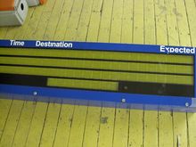
In upstairs metalworking there is a train station display - photos on flickr. The display was acquired in October 2011 and hasn't been set up to do anything yet.
The display seems to use 4-wire MODBUS, and has some DIP switches to configure it's ID (currently 20, as displayed at startup). The registers and commands will be completely undocumented, so bitbanging the display seems like an easier idea.
The intention is to display messages from discord (and will be named dispcord accordingly). The time section at the bottom will display the channel name, and the main three lines will show the sender and preview of the message. The Discord bot already relays messages from non-private channels to MQTT.
Parts
LED Module
Each LED module contains an 8x7 grid of LEDs. It looks like the module could take 8x8, but maybe the font used wouldn't benefit from having an extra row.
The cathodes of each column are connected together, and the anodes of each row are connected together. At the top and bottom of each module, there is a set of 12 male pins which interface with the module backplane.
p4 n n p3 n n p2 n n p1 n n

o o o o o o o o      row 1 (via p1 top)
o o o o o o o o      row 2 (via p2 top)
o o o o o o o o      row 3 (via p3 top)
o o o o o o o o      row 4 (via p4 top)

o o o o o o o o      row 1 (via p1 bottom)
o o o o o o o o      row 2 (via p2 bottom)
o o o o o o o o      row 3 (via p3 bottom)
x x x x x x x x      row 4 (via p4 bottom, not populated)

p4 n n p3 n n p2 n n p1 n n
LED Module Backplane
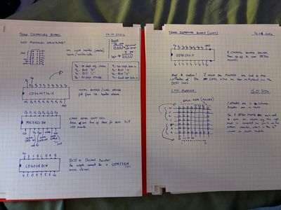
Each backplane holds 8 LED modules. There is a 14 pin IDC header on the right of each board, these go to a CD74HCT541E octal buffer.
Input IDC header

   solder side                             header side
     +-----+                                  +-----+
GND -| o o |- A0                         GND -| o o |- A6  Strobe
GND -| o o |- A1              Shift2 Di  A7  -| o o |- A5  BCD D
GND -| o o |- A2                         GND -| o o |- A4  BCD C
?   -| o o |- A3                         ?   -| o o  - A3  BCD B
GND -| o o |- A4                         GND -| o o |- A2  BCD A
 A7 -| o o |- A5                         GND -| o o |- A1  Shift1 Di
GND -| o o |- A6                         GND -| o o |- A0  Clock
     +-----+                                  +-----+

(I'm bad at geometry and will get confused :))

CD74HCT541E

    V O
    c E Y Y Y Y Y Y Y Y     <---- outputs
    c 2 0 1 2 3 4 5 6 7
  +---------------------+
  |>   CD74HCT541E      |
  +---------------------+
    O A A A A A A A A G
    E 0 1 2 3 4 5 6 7 N     <--- inputs
    1                 D
Some of the output lines from the line driver go to the shift registers, while others go to a BCD decoder. Each LED Module has two shift registers which are both updated on each clock pulse.
CD74HCT541E Outputs

Y0 - All shift registers, CLOCK
Y1 - Bottom shift register of right-most LED Module, Data In
Y2 - BCD Decoder "A"
Y3 - BCD Decoder "B"
Y4 - BCD Decoder "C"
Y5 - BCD Decoder "D"
Y6 - All shift registers, STROBE
Y7 - Top shift register of the right-most LED Module, Data In
The shift registers used are CMOS MIC5821BN
MIC5821BN

     O O O O O O O O
     1 2 3 4 5 6 7 8
   +-----------------+
   |> MIC5821BN      |
   +-----------------+
     C S V V S S O V
     L i s d o T E e
     K   s d   B   e

Vss, OE and Vee are all tied to ground.
Si is serial in and connects to either Y1 or Y2 of the line driver, or to So of the previous shift register.

The BCD decoder (CD4028BCN) is used to turn on/off the columns of all LED modules on an LED module backplane, using a MOSFET (IRF540) and octal source driver UDN2981A.

    V
    d
    d 3 1 B C D A 8
  +-----------------+
  |>  CD4028BCN     |
  +-----------------+
    4 2 0 7 9 5 6 V
                  s
                  s

                    G
    O O O O O O O O N
    0 1 2 3 4 5 6 7 D
  +-------------------+
  |>  UDN2981A        |
  +-------------------+
   I I I I I I I I V
   0 1 2 3 4 5 6 7 s
Backplane Frame
Each LED Module Backplane is arranged on the backplane frame.
The backplanes are grouped into two. The first group drives 6x8 LED Module backplanes (total of 2688 LEDs) and the second drives 4x8 LED Module backplanes (1792 LEDs). In total there are 4480 LEDs per side.
+------------------+------------------+------------------+
|  A2              |  A1              |   A0             |  <--- Input
+------------------+------------------+------------------+
|  A5              |  A4              |   A3             |
+------------------+------------------+------------------+
|  B2              |  B1              |   B0             |  <--- Input
+------------------+------------------+------------------+
                   |  B3              |
                   +------------------+
Bit banging...
Not had much luck with this yet, but I'm not sure why.
Logic analyzer trace of data lines during power on boot message (can be opened with PulseView) File:Train Departure Board Logic Dump.zip. Screenshot for convenience below
Note: In the screenshot it looks like single clock pulses, but each one of those is 8 pulses. Each clock pulse is about 500ns. Arduino using the IO registers is about 250ns, but this is within the timing recommendations for the shift registers, and I've tried reducing the speed too.
Unanswered and confusing questions
- Why do the two shift registers always receive the same data? My understanding is that one register does the top four rows, and one register does the bottom three rows, but they seem to receive the same data. Very confusing
- Why can't I even get an LED to light up? I leave the shift register data in lines high, multiplex the BCD lines, pulse the clock, do the strobe in the right place (or just leave it high).
- Why does the BCD "D" line only stay high for 68us? And why is it pulsed after each 48 clock pulses? (48 presumably because there are six sets of 8 LED boards?)
- the supposed D line does not increment like the other lines, looking at it again. I'm starting to suspect I've mixed up one or two lines - I don't think there needs to be a D line since we are counting from 0-7 (for the 8 columns). I will check the pin out and where they are connected again.
This is my crappy code so far.
// PORTD
// n/a   |  n/a  | STROBE | CLOCK | SHIFT A DATA IN | SHIFT B DATA IN | n/a | n/a

#define ALL_STROBE        B00000100
#define ALL_CLOCK         B00001000
#define FIRST_SHIFT_DATA  B00010000
#define SECOND_SHIFT_DATA B00100000

// PORT B (just doing the four BCD lines)

void setup() {
  DDRB = DDRB | B11111111;
  DDRD = DDRD | B00111100;
}

char column = 0;

void loop() {
    // Turn on the strobe
  for (int i=0; i < 100; i++)
    PORTD = (PORTD | ALL_STROBE);

  // Clock out 64 bits of data
  for (int i=0; i < 64; i++) {
    // Currently leaving these set high.
    if ((i % 2) == 0) {
      PORTD = PORTD | FIRST_SHIFT_DATA;
      PORTD = PORTD | SECOND_SHIFT_DATA;
    } else {
      PORTD = PORTD & ~FIRST_SHIFT_DATA;
      PORTD = PORTD & ~SECOND_SHIFT_DATA;
    }

    // Pulse the clock
    for (int d=0; d < 5; d++) PORTD = PORTD | ALL_CLOCK;
    PORTD = PORTD & ~ALL_CLOCK;
  }


  PORTB = column & ~8;
  if (column > 7) column = 0;

  // Pulse the BCD D line for no reason
  for (int i=0; i < 50; i++) {
    PORTB = PORTB | 8;
  }
  PORTB = PORTB & ~8;

   // Turn off the strobe
  for (int i=0; i < 100; i++)
    PORTD = PORTD & ~ALL_STROBE;

  column++;
}

